
The next stage of the refurbishment process comprises the following actions:
- Final memory upgrade to make use of the full 32KB provided by the CY62256NLL module.
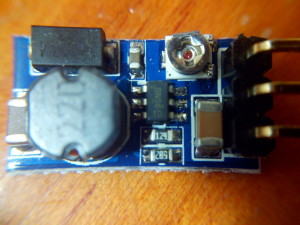
- Replacement of the original LM7805 linear voltage regulator by a switching regulator.
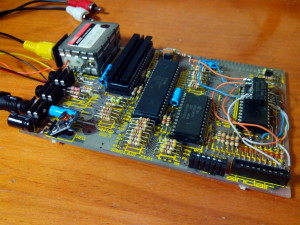
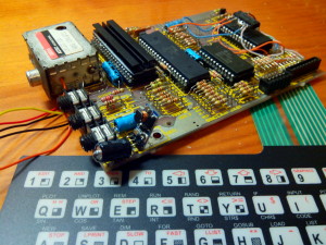
- Miscellaneous minor modifications such as the installation of a keyboard membrane, rubber pads and case screws, and final cleanup of contacts and case.
Once again, the memory upgrade has been undertaken following the guidelines shown in the following URL. This modification is based upon the use of two of the logical NAND gates in a 74LS00 component.
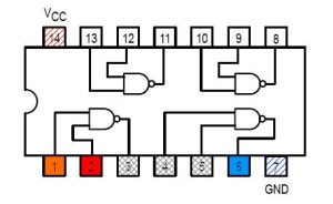
As shown in the schematic above, pin 1 in the 74LS00 IC (shown in orange) will be connected to the board track which connects the ULA with pin 22 (top side) in the edge connector (/M1 signal). Pin 2 (shown in red color) will be connected with the cathode of D8 diode (line A15). The output of this logical gate, located in Pin 3, will be connected to the two inputs (Pins 4 and 5) in the logical gate right ahead (the three pins are shown in dashed gray above). The output of this logical gate, located in Pin 6 (shown in blue above), will be connected with Pin 1 in the CY62256NLL SRAM module which, up until this moment and as detailed in the former blog entry, was connected to GND. This connection to GND needs to be now removed to ensure proper functioning of the memory upgrade. The two remaining connections in the 72LS00 IC are the connection to GND through Pin 7, and the connection to the 5V rail through Pin 14 which are necessary for the operation of the IC.
The 74LS00 IC is placed on top of the CYL62256NLL SRAM module, separated by a rubber pad which prevents both ICs from getting in contact with each other, while at the same time estabilizing its placement.
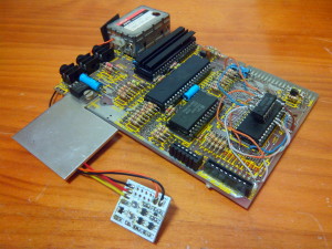
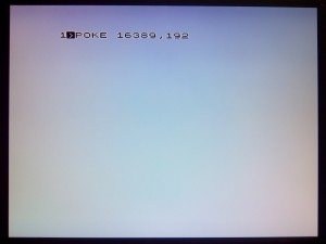
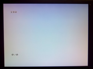
The next part of this stage of the refurbishment process considers the removal of the LM7805 linear voltage regulator and its heat sink. The removal of the original components, and the installation of the switching regulator are fairly straightforward as the new component is typically supplied as a drop in replacement with the same configuration, footprint, and pin arrangement.
The installation of the switching regulator will ensure a much better efficiency and less dissipated heat, allowing for the removal of the original heat sink. The new switching regulator also provides, as was the case with the original linear regulator, appropiate thermal and short circuit protection. The main drawback of this particular modification would be a lower allowable current which is established at 1A for this particular switching regulator; in any case, this value falls within the expected nominal values in this configuration.
Go back to Part I.