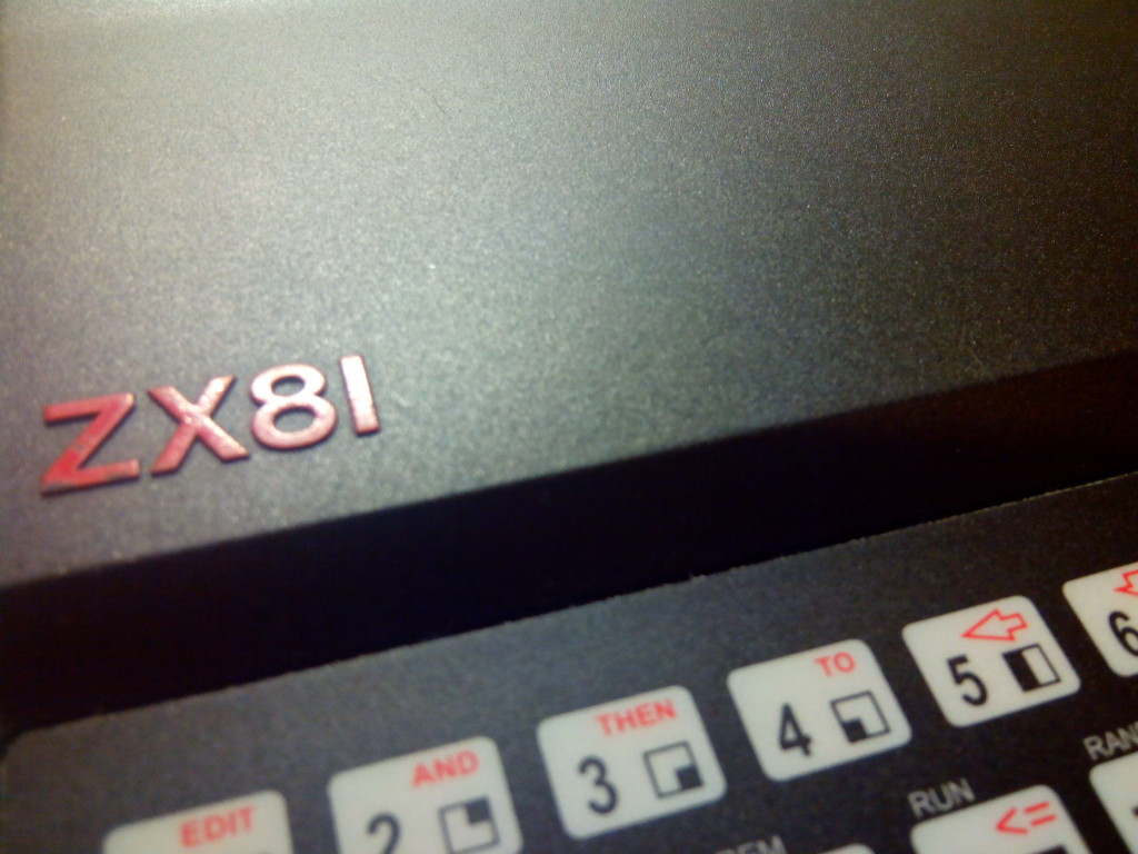
The computer being refurbished is a ZX81, released in 1981 by Sinclair Research as a follow up to the ZX80 model, both computers enjoying a great deal of success in the UK mostly due to its low cost and general availability.
The purpose of the refurbishment process is twofold: on the one hand, to address specific issues particular to this unit, such as a broken keyboard membrane; on the other hand, to replace certain components with the end goal of increasing the life of the unit.
The refurbishment process will account for the following actions:
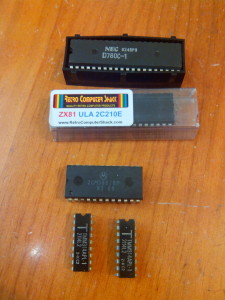
- Replacement of the original ULA, version 2C184E, by a more recent component, version 2C210E, which also addresses the lack of back porch signal in the old version.
- Installation of a heat sink on top of the new ULA, due to the relatively high service temperature and so as to increase the life of this component.
- Installation of the ZX81CCB board which works up the video signal and removes noise, while also introducing a back porch signal regardless of the ULA version installed onboard. In addition, the computer is fitted with composite video ouput.
- Installation of an internal RAM upgrade to a full 32KB by means of a CY62256NLL module, a high performance CMOS static ram with low power requirements.
- Replacement of the original NEC Z80 processor by a low power CMOS Zilog Z84C processor.
- Replacement of the LM7805 linear voltage regulator by a switching regulator suitable for 5V and 1A, resulting in an increase of efficiency and allowing for the removal of the existing aluminum heat sink.
- Replacement of the original ROM by an ASZMIC assembly development environment.
From a functional point of view, the following actions will be identically undertaken:
- Installation of a new keyboard membrane.
- Cleaning of PCB contacts.
- Installation of rubber pads and missing screws.
The refurbishment process will be split in two blog entries, the first one being focused in the aforementioned actions except for the installation of the switching regulator and the last stage of the memory upgrade, which will be initially upgraded to 16KB only.
The material required for the first stage of this refurbishment process would be as follows:
- 1x Zilog Z84C0006PEG CPU.
- 1x Ferranti 2C210E ULA.
- 1x SRAM Cypress CY62256NLL 256-KBit (32KB x 8).
- 1x PROM 2364 ASZMIC.
- 1x ZX81CCB Board.
- 1x Switching voltage regulator, output rating 5V @1A.
- 1x 40 pin heat sink.
- 1x 40 pin socket (CPU).
- 1x 28 pin socket (SRAM).
- Electrical wires.
- Thermal paste.
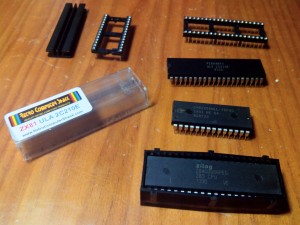
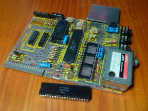
The original ULA IC is carefully removed so as to avoid damaging the component. A new 40 pin socket is installed, and the new 2C210E ULA is fitted with the heat sink resting on top of a layer of thermal paste.
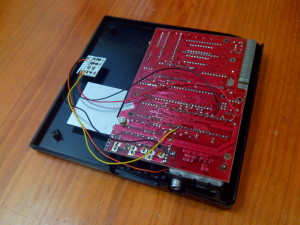
The ZX81CCB wires are soldered to the appropriate locations as detailed in the instructions manual; this is done on the back side of the main board (opposite to the component side). The ZX81CCB would typically require some manual tuning so as to ensure that it is set to the appropriate ULA version which has just been installed. This is properly explained in the instructions manual.
The next step of the process is the memory upgrade, following the steps shown in the following URL.
The two existing 2114 ICs are carefully removed so as to ensure they can be reused in future projects. A new 28 pin socket is installed in the position marked as IC4 in the main board. In addition, an existing jumper marked as LK2 and located right next to IC4 needs to be closed by means of a small wire. We can now install the SRAM CY62256NLL IC on the socket, bending five of its pins (1, 2, 22, 23 y 26) up so as to ensure they do not make contact with the socket and board pads underneath. These five pins will be connected to the following locations: GND, D3 cathode, GND, D1 cathode and D5 cathode, respectively.
Pin 27 and pin 28 of the SRAM module can be connected through a 10K ohm resistor so as to activate the HRG8 mode.
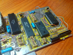
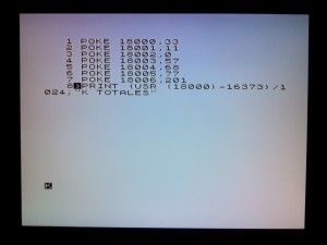
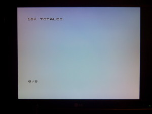
Having verified the proper functioning of the memory upgrade, the NEC Z80 CPU is carefully removed, and a new 40 pin socket is soldered in to facilitate the installation of the new Zilog Z84C processor. Finally, the original Sinclair ROM IC is replaced by the ASZMIC PROM.
The pictures below show the overall appearance of the board, with the new components fitted on the sockets and with the heat sink fitted on the ULA. Once again, and as previously discussed, all the components which have been removed from the board will be stored safely so as to be reused in other projects.
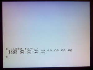
A final functional verification of the board is undertaken and the upgraded components are found to be in good working order.
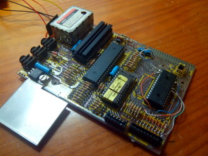
The next blog entry will cover the removal of the LM7805 linear voltage regulator and its heat sink, as well as the installation of the switching regulator. The final memory upgrade will be identically undertaken, resulting in a total memory capacity of 32KB.
Continue to Part II.